Research Highlights
GeSn Material Characterization & Devices Fabrication
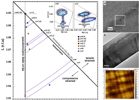
Reciprocal Space Map sketch with measured reciprocal lattice points of 0.9-7% Sn films. Top two images show RSM images of samples with Sn% of 06% and 7%. a) High Resolution TEM image of Ge/GeSn interface and misfit dislocations, b) TEM image of Si/Ge/Ge.93Sn.07 film, c) AFM image of Ge.93Sn.07 sample with cross-hatch patterns that shows relaxation mechanisam in GeSn overlayer.
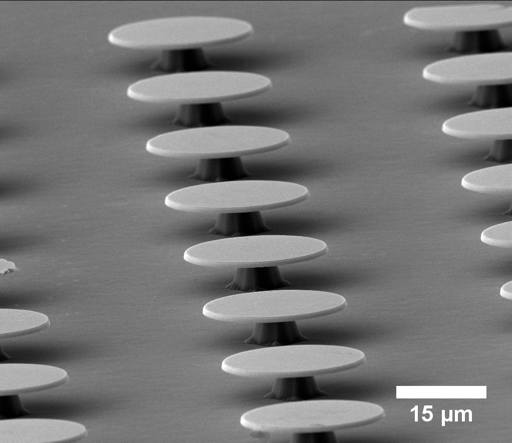
GeSn microdisk: GeSn microdisks integrated on Si. The microdisks were patterned using standard optical photolithography methods followed by reactive ion etching. The Si post was formed by wet etching process. The whispering-gallery-modes (WGMs) were observed, which indicate the achievability of lasing with an optimized disk structure.
The temperature dependent spectral response of each photoconductor was measured, and a maximum long wavelength response to 2.1 μm was observed for the 7.0% Sn sample. The DC responsivity measured at 1.55 μm showed around two orders of magnitude improvement at reduced temperatures for all samples compared to room temperature measurements. The noise current and temperature dependent specific detectivity (D*) were also measured for each sample at 1.55 μm, and a maximum D* value of 1 × 109 cm·√Hz/W was observed at 77 K.
Fabrication Structures Using EBL
Fabrication of metallic fishnet structure integrated (on top) Schottky contact a-Si solar cell with Aluminum as back contact.
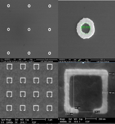
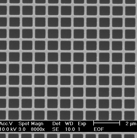
SEM images of a structure processed by EBL.
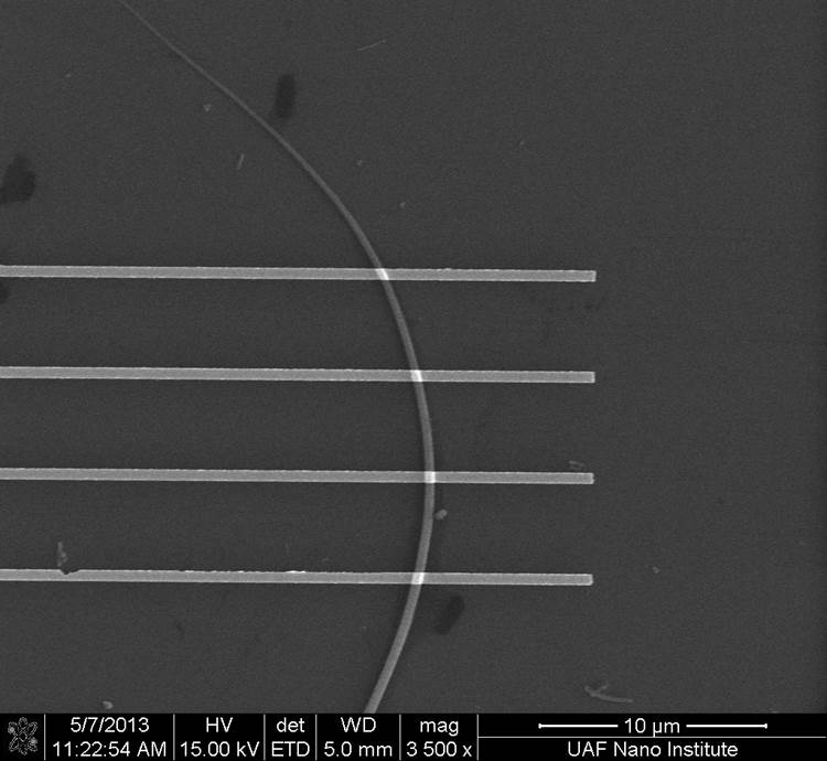
Fabrication of single Si nanowire device.